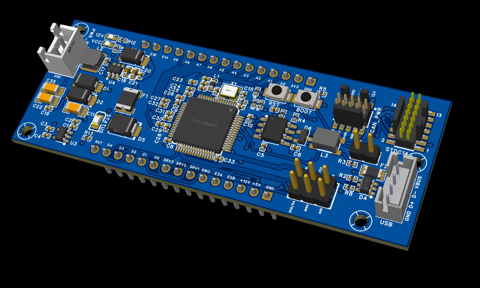
One board, two roles
The PRD-NODE is the universal building block of the Park Road Designs ecosystem. It serves as both a peripheral node — plugging into a breakout board to drive an instrument or control group — and as the CAN-USB bridge for the whole rig.
Two population variants define the role. As a peripheral node, pin headers are soldered and the board plugs onto a breakout board. As a bridge, the USB connector, barrel jack connector, and CANTERM jumper are populated instead — no headers needed, and no separate bridge hardware to design or buy.
The board exposes 30 user pins across two rows of 15, plus a dedicated SPI2 2×3 header for displays and SPI peripherals. Every function of the STM32F072RBT6 that matters for flight sim peripherals is brought out.
One NODE per instrument group. Pair with a breakout board for trim and flaps, another for the throttle quadrant, another for a radio panel. All talk CAN bus over Ethernet cables.
Key Highlights
| MCU | STM32F072RBT6 Cortex-M0 @ 48MHz |
| Flash / RAM | 128KB / 16KB SRAM |
| PCB | 80×30mm 4-layer FR4 |
| ADC | 10 × 12-bit (A0–A9) |
| Hardware encoders | 3 × quadrature (TIM2/3/4) |
| Servo PWM | 3 × TIM1_CH1-3 (50Hz) |
| User headers | 2 × 15-pin 2.54mm |
| SPI2 header | 2×3 2.54mm (SCK/MOSI/MISO/CS) |
| CAN bus | 500kbps via TJA1051T/3 |
| USB | CDC SLCAN (bridge mode) |
| Power input | 12V via CAN IDC or barrel jack connector |
| Debug | STDC14 (proto only, DNP production) |
Same board, two configurations
🧩 Peripheral Node
| 2×15 pin headers | ✓ Populated |
| SPI2 2×3 header | ✓ Populated |
| CAN_PWR IDC connector | ✓ Populated |
| STDC14 debug | Prototype only |
| USB connector | — DNP |
| Barrel jack connector (CN1) | — DNP |
| CANTERM jumper | — DNP |
🌉 Bridge
| USB connector (PH2.0-4P) | ✓ Populated |
| Barrel jack connector (CN1) | ✓ Populated |
| CANTERM jumper | ✓ Fitted |
| CAN_PWR IDC connector | ✓ Populated |
| STDC14 debug | Prototype only |
| 2×15 pin headers | — DNP |
| SPI2 header | — DNP |
The bridge NODE mounts in an enclosure with panel-mount USB (to PC), panel-mount RJ45 (to CAN bus), and a panel-mount barrel jack (12V input). CN1 is a 2-pin XH connector wired to the barrel jack with two wires. Total BOM addition: three connectors.
Electrical
| Supply (12V) | 8–16V via CAN IDC or CN1 barrel jack connector |
| 3V3 rail | 500mA max (TPRT9013-33GB LDO) |
| 5V rail | ~4.7V post Schottky (AP63205WU-7 buck) |
| 12V polyfuse F1 | 2A hold / 4A trip (1812L200/30GR) |
| USB polyfuse F2 | 500mA hold / 1A trip |
| GPIO logic | 3.3V (5V tolerant on most pins) |
| ADC reference | VDDA = 3.3V |
| ADC resolution | 12-bit (0–4095) |
Mechanical
| PCB dimensions | 80mm × 30mm |
| PCB layers | 4-layer (L1 signal, L2 GND, L3 power, L4 signal) |
| Mounting holes | 4× NPTH corner holes (no net) |
| User headers | 2 × 15-pin 2.54mm through-hole |
| SPI2 header | 2×3 2.54mm through-hole |
| CAN_PWR IDC | 14-pin 1.27mm SMD (FTSH-107) |
| STDC14 | 14-pin 1.27mm SMD (DNP production) |
| Crystal | 16MHz X322516MLB4SI |
CAN Bus
| Standard | CAN 2.0B (ISO 11898) |
| Transceiver | TJA1051T/3 (NXP) 3.3V |
| Bit rate | 500kbps |
| Termination | CANTERM1 2-pin 2.54mm header jumper |
| ESD | PESD2CAN SOT-23 |
| EMI filter | ACT45B CMC |
| Bus cable | Standard straight-through Ethernet (custom RJ45 pinout) |
USB
| Standard | Full Speed USB 2.0 |
| Device class | CDC Virtual COM port (SLCAN) |
| Bridge trigger | VBUS sense on PC14 |
| ESD | USBLC6-2SC6 SOT-23-6 |
| Connector | PH2.0-4P THT (DNP peripheral) |
Some pins show their alternate function name on the NODE silkscreen rather than a friendly name. Key mappings: SIG1 = SRV2 (PA9/USART1_TX), SWO = ENC2 push button (PB3), SW1 = ENC1 push button (PA15). Both PA15 and PB3 require JTAG remap in firmware before use as GPIO.
Row 1 — Top (Analog & Encoders)
Pins 1–2 power, pins 3–12 analog ADC, pins 13–15 hardware encoders.
| Pin | Label | GPIO | Primary | Alt function |
|---|---|---|---|---|
| 1 | GND | — | Ground | |
| 2 | VCC | — | 3.3V regulated | |
| 3 | A0 | PA0 | ADC CH0 | TIM2_CH1 |
| 4 | A1 | PA1 | ADC CH1 | TIM2_CH2 |
| 5 | A2 | PA2 | ADC CH2 | TIM2_CH3 |
| 6 | A3 | PA3 | ADC CH3 | TIM2_CH4 |
| 7 | A4 | PA4 | ADC CH4 | DAC1 output |
| 8 | A5 | PA5 | ADC CH5 | DAC2 output |
| 9 | A6 | PA6 | ADC CH6 | TIM3_CH1 PWM |
| 10 | A7 | PA7 | ADC CH7 | TIM3_CH2 PWM |
| 11 | A8 | PB0 | ADC CH8 | TIM3_CH3 PWM |
| 12 | A9 | PB1 | ADC CH9 | TIM3_CH4 PWM |
| 13 | E1A | PB4 | TIM3 Encoder A | Hardware quadrature |
| 14 | E1B | PB5 | TIM3 Encoder B | Hardware quadrature |
| 15 | E2A | PB6 | TIM4 Encoder A | Hardware quadrature |
Row 2 — Bottom (Digital, Servo, Encoders)
Pins 1–3 power, pins 4–9 encoder/servo signals, pins 10–14 digital GPIO, pin 15 reset.
| Pin | Label | GPIO | Primary | Alt / Notes |
|---|---|---|---|---|
| 1 | GND | — | Ground | |
| 2 | +5V | — | ~4.7V regulated | |
| 3 | +12V | — | 12V (when 12V supply present) | |
| 4 | E2B | PB7 | TIM4 Encoder B | Hardware quadrature |
| 5 | SW1 | PA15 | GPIO (ENC1 button) | ⚠ JTAG pin — needs remap in firmware |
| 6 | SWO | PB3 | GPIO (ENC2 button) | ⚠ JTAG pin — needs remap in firmware |
| 7 | SRV1 | PA8 | TIM1_CH1 50Hz PWM | Primary servo output |
| 8 | SIG1 | PA9 | TIM1_CH2 PWM | USART1_TX alt — SRV2 signal |
| 9 | USART1_RX | PA10 | TIM1_CH3 PWM | SRV3 signal |
| 10 | SW3 | PB2 | GPIO (D0) | — |
| 11 | SW4 | PB10 | GPIO (D1) | I2C2_SCL |
| 12 | SW5 | PB11 | GPIO (D2) | I2C2_SDA |
| 13 | SW6 | PB12 | GPIO (D3) | SPI2_NSS |
| 14 | D4 | PB13 | GPIO | SPI2_SCK — also on SPI2 header |
| 15 | RST | NRST | Reset | — |
Dedicated SPI2 Port
A 2×3 2.54mm header breaks out the full SPI2 peripheral — SCK, MOSI, MISO, CS, plus 3V3 and GND. This exposes PB14 (MISO) and PB15 (MOSI) which are not available on the main headers.
PB12 (CS) and PB13 (SCK) are dual-exposed — also accessible on the main headers as SW6 and D4. Using SPI2 for a display doesn't consume any other header pins.
Physical layout
| Pin | Signal | GPIO | MCU Pin |
|---|---|---|---|
| 1 | SCK / D4 | PB13 | 26 |
| 2 | MOSI | PB15 | 28 |
| 3 | CS / D3 | PB12 | 25 |
| 4 | MISO | PB14 | 27 |
| 5 | GND | — | — |
| 6 | 3V3 | — | — |
Use cases
Connect SCK, MOSI, CS directly. DC and RST use spare GPIO (e.g. SW3, SW4). MISO not required for this write-only display but available for other peripherals. Max SPI clock: 10MHz.
Same connection as SSD1322. Alternatively use SSD1306 in I2C mode via D1/PB10 (I2C2_SCL) and D2/PB11 (I2C2_SDA) — no SPI2 header needed.
The full MOSI/MISO/SCK/CS port supports any SPI device — shift registers, ADCs, DACs, flash memory. Multiple CS devices can share MOSI/MISO/SCK with separate CS lines from spare GPIO pins.
PB12–PB15 map to consecutive MCU pins on the LQFP-64, making routing from the MCU to the SPI2 header very clean with no crossing traces.
Power Architecture
The PRD-NODE receives 12V from the CAN bus via the CAN_PWR IDC connector. The AP63205WU-7 buck converter produces 5V, which feeds the TPRT9013-33GB LDO for 3.3V. All three rails are available on the pin headers for breakout board use.
The 12V_IN net receives power from: CAN_PWR IDC pins 6/8/11, and CN1 barrel jack connector pin 1 (when populated for bridge use). Both feed the same net upstream of F1 polyfuse.
Power rail table
| Rail | Source | Header pin | Notes |
|---|---|---|---|
| +12V | CAN bus / CN1 | Row 2 pin 3 | Present only when 12V connected |
| +5V | AP63205WU-7 buck | Row 2 pin 2 | ~4.7V post Schottky OR diode |
| 3V3 / VCC | TPRT9013-33GB LDO | Row 1 pin 2 | 3.3V regulated 500mA max |
Protection
| F1 — 12V polyfuse | 1812L200/30GR — 2A hold, 4A trip, 30V |
| F2 — USB polyfuse | SMD1206-050-16 — 500mA hold, 1A trip |
| D5 — TVS | SMBJ15A DO-214AA on 12V input |
| D4 — USB ESD | USBLC6-2SC6 SOT-23-6 |
| D6 — CAN ESD | PESD2CAN SOT-23 |
| Schottky OR | SS34 ×2 — seamless 12V/USB switchover |
The Schottky OR circuit allows simultaneous USB and 12V connection with no issues. USB provides VBUS for bridge detection; 12V powers the CAN bus and breakout boards.
CAN Bus Network
Connect PRD-NODE boards via standard straight-through Ethernet patch cables. The RJ45 connectors use a custom pinout — do not connect to Ethernet equipment.
RJ45 connectors carry CAN bus signals and 12V DC on pins 4–5. Connecting to network switches or routers will damage both the PRD-NODE and the network equipment.
RJ45 Custom Pinout
| Pin | Signal |
|---|---|
| 1 | CAN_H |
| 2 | CAN_L |
| 3 | GND |
| 4–5 | +12V power |
| 6–8 | GND |
Bus Settings & Termination
Fit the CANTERM1 jumper only on the two physical end nodes of the CAN bus chain.
| Bridge NODE (always an endpoint) | Jumper FITTED |
| Middle peripheral NODEs | Jumper REMOVED |
| Last peripheral NODE in chain | Jumper FITTED |
Prescaler: 6 — BS1: 11TQ — BS2: 4TQ — SJW: 1TQ
The 14-pin FTSH-107 IDC connector carries CAN_H, CAN_L, and 12V/GND to the NODE from the RJ45 board. Uses centre 10 pins — pins 3–12. Outer 4 pins are NC.
Bridge Configuration
A bridge-configured PRD-NODE replaces the legacy PRD_USBCAN_MB board. No separate bridge board is required — just populate the three connectors on a standard NODE and mount it in an enclosure.
Required connections
| CN1 (barrel jack) | HX-XH2.54-2PZZ-R 2-pin XH → panel-mount 2.1/5.5mm barrel jack. Pin 1 = +12V, Pin 2 = GND. |
| USB connector | PH2.0-4P → panel-mount USB (to PC). No driver required — CDC SLCAN. |
| CAN_PWR IDC | IDC ribbon cable → existing RJ45 board. Distributes 12V to CAN bus via RJ45. |
| CANTERM1 | Jumper fitted — bridge is always a bus endpoint. |
No firmware changes. When VBUS is detected on PC14, the NODE automatically enters CDC SLCAN bridge mode. Unplug USB and it returns to normal peripheral behaviour.
Enclosure Requirements
Mount the bridge NODE in any small enclosure with three panel cutouts:
| Barrel jack hole | 8mm round (2.1/5.5mm centre-positive) |
| RJ45 hole | 14×20mm standard RJ45 panel cutout |
| USB hole | 8×7mm (USB-B) or 9×4mm (USB-C) |
Barrel jack (+12V) → CN1 pin 1 → 12V_IN net → F1 polyfuse → SMBJ15A protection → AP63205 buck → NODE power rails. The same 12V also distributes to the CAN bus via the RJ45 board.
Connect 12V to either the barrel jack (bridge) OR via the CAN bus from another bridge — not both simultaneously.